Semiconductor Wafer Level Manufacturing Equipment

Forces Driving Semi Mergers Acquisitions Ee Times Semiconductor Semiconductors Merger

Inspecting Unpatterned Wafers

Semiconductor

Advantest M6761ad Dynamic Test Handler For Sale Jmc Worldwide Semiconductor Equipment Semiconductor Semiconductor Manufacturing Test

Fine Tuning Chemical Mechanical Polishing Head With Fuji Prescale Film Keywords Wafer Polishing Semiconductor Production Cmp Semiconductor Mechanic Repair
Semiconductor Wafer Metrology Tools Compare Review Quote Buy

Wafer level packaging wlp is becoming an important semiconductor packaging technology.
Semiconductor wafer level manufacturing equipment.

Silicon Wafers Producers And Suppliers Company Semiconductor Materials Low Stress Semiconductor

Semiconductor Wafer Processing Ic Packaging Testing Solutions Leica Microsystems

Semiconductor Wafer Cleaning Equipment Market Report Ability
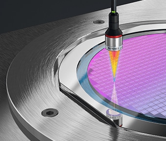
Semiconductor Wafer And Glass Substrates Inspection Inspection Methods For Quality Assurance Coating Dispensing Technology Keyence America

30941 Wafer Sorter Robotic Engineering Tal82c For Sale At Bmisurplus Com Robotics Engineering Equipment For Sale Engineering

Acm Research Expands Suite Of Semi Critical Cleaning Systems

Semiconductor Metrology System For Wafer Flatness Measurement Inspection

Pin By Tes Clean Air Systems On Fan Filter Units Mac 10 Clean Air Filters

Pin On Pvateplaamerica Com
Global Wafer Fab Equipment Revenue By Maker 2018 Statista

Industrial Chip Market On A Roll Electronics Weekly Marketing Industrial Semiconductors
Gas Delivery S Role In Semiconductor Wafer Creation

Junhe Double Group Silicon Slice Detergent Jh 1015 Brief This Is Patent Products For Degreasing Electron Level And Solar G Patented Products Cleaning Metal Ion

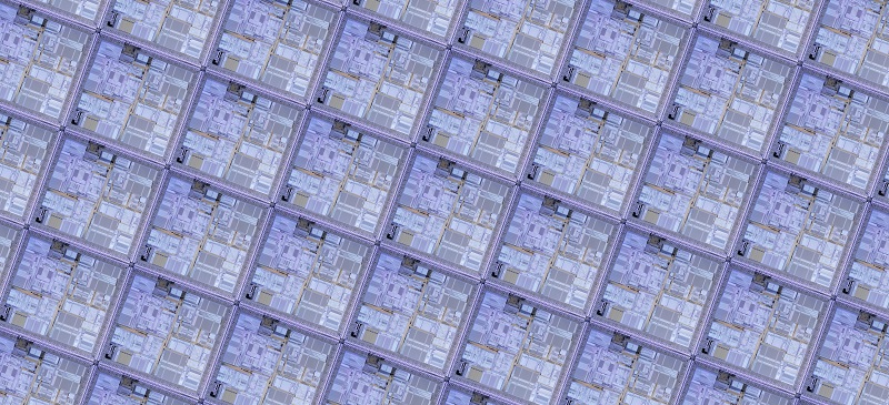
From Sand To Silicon The Making Of A Chip We Are Intel Sand Intel Semiconductor
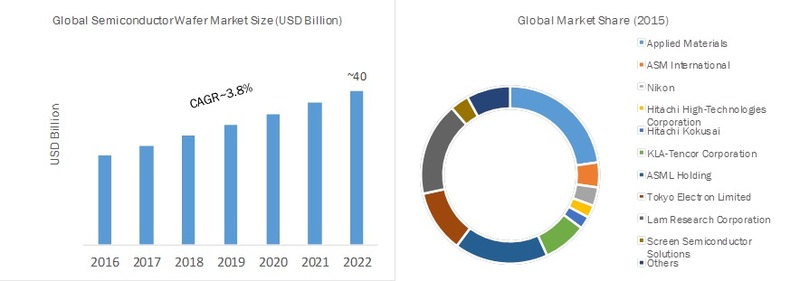
Global Semiconductor Wafer Market Research Report Forecast 2022
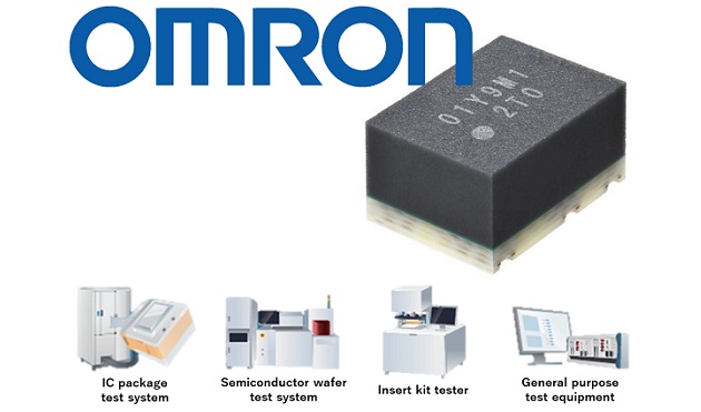
World S First Mosfet Relay Introduced For Semiconductor Wafer Test System Ele Times

Additive Manufacturing For Semiconductor Devices And Its Impact On R D

2018 Global Semiconductor Equipment Sales Were Record 64 5b Evaluation Engineering
Https Encrypted Tbn0 Gstatic Com Images Q Tbn 3aand9gcsvtra Yd3hz9k5q4foguz0eru Avnnz2dainias1s Usqp Cau

Pin On Semiconductors

If You Have An Equipment Without Gem Secs Capability And If You Can T Get It From The Oem We Can Help You Einn Linux Operating System Gems Operating System

Acm Research Launches Stress Free Polishing Tool For Advanced Packaging Applications Delivers First Tool To Leading Chinese Osat News

Pin On Semiconductors

Modular Semiconductor Clean Rooms For Wafer Fabrication
Source : pinterest.com
